- 您现在的位置:买卖IC网 > Sheet目录1905 > ATMEGA324PA-MCHR (Atmel)MCU AVR 32KB FLASH 20 MHZ 44QFN
PIC16C925/926
DS39544A-page 142
Preliminary
2001 Microchip Technology Inc.
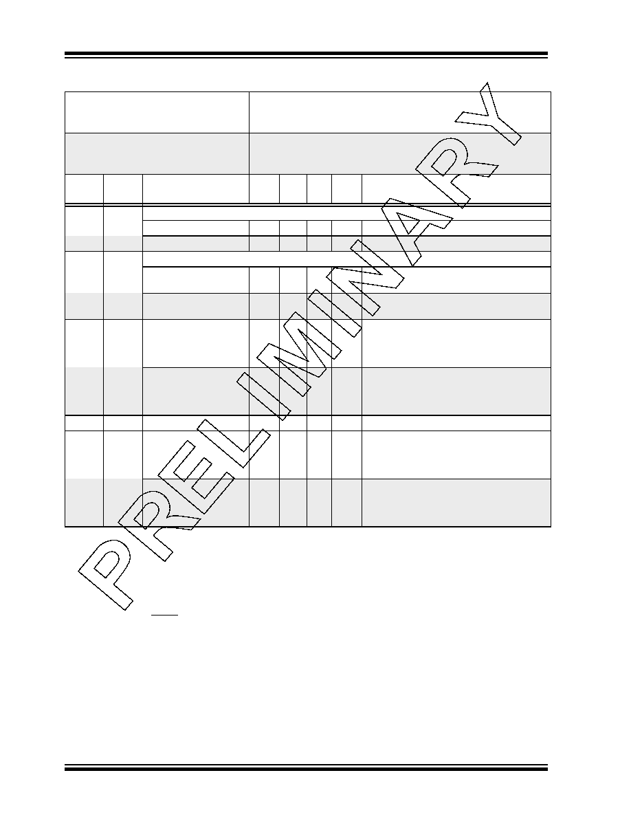
IPD
Power-down Current (Note 3)
D020
PIC16LC925/926
—
0.9
5
AVDD = 3.0V
D020
PIC16C925/926
—
1.5
21
A
VDD = 4.0V
Module Differential Current (Note 5)
D021
IWDT
Watchdog Timer
PIC16LC925/926
—
6.0
20
AVDD = 3.0V
D021
Watchdog Timer
PIC16C925/926
—
9.0
25
A
VDD = 4.0V
D022
ILCDT1
LCD Voltage
Generation with
internal RC osc enabled
PIC16LC925/926
—
36
50
AVDD = 3.0V (Note 7)
D022
LCD Voltage
Generation with
internal RC osc enabled
PIC16C925/926
—
40
55
A
VDD = 4.0V (Note 7)
D022A
IBOR
Brown-out Reset
—
100
150
A
BODEN bit set, VDD = 5.0
D024
ILCDT1
LCD Voltage
Generation with
Timer1 @ 32.768 kHz
PIC16LC925/926
—
15
29
AVDD = 3.0V (Note 7)
D024
LCD Voltage
Generation with
Timer1 @ 32.768 kHz
PIC16C925/926
—
33
60
A
VDD = 4.0V (Note 7)
15.1
DC Characteristics
(Continued)
PIC16LC925/926
(Commercial, Industrial)
Standard Operating Conditions (unless otherwise stated)
Operating temperature
-40°C
≤ TA ≤ +85°C for industrial
0°C
≤ TA ≤ +70°C for commercial
PIC16C925/926
(Commercial, Industrial)
Standard Operating Conditions (unless otherwise stated)
Operating temperature
-40°C
≤ TA ≤ +85°C for industrial
0°C
≤ TA ≤ +70°C for commercial
Param
No.
Sym
Characteristic
Min
Typ Max Units
Conditions
Data in "Typ" column is at 5V, 25°C unless otherwise stated. These parameters are for design guidance only
and are not tested.
Note 1: This is the limit to which VDD can be lowered in SLEEP mode without losing RAM data.
2: The supply current is mainly a function of the operating voltage and frequency. Other factors such as I/O pin load-
ing and switching rate, oscillator type, internal code execution pattern, and temperature also have an impact on
the current consumption.The test conditions for all IDD measurements in active operation mode are:
OSC1 = external square wave, from rail to rail;
all I/O pins tri-stated, pulled to VDD
MCLR = VDD.
3: The power-down current in SLEEP mode does not depend on the oscillator type. Power-down current is
measured with the part in SLEEP mode, with all I/O pins in hi-impedance state and tied to VDD and VSS.
4: For RC osc configuration, current through REXT is not included. The current through the resistor can be esti-
mated by the formula Ir = VDD/2REXT (mA) with REXT in kOhm.
5: The
current is the additional current consumed when this peripheral is enabled. This current should be
added to the base IDD or IPD measurement.
6: PWRT must be enabled for slow ramps.
7:
ΙLCDT1 and ΙLCDRC includes the current consumed by the LCD Module and the voltage generation
circuitry. This does not include current dissipated by the LCD panel.
发布紧急采购,3分钟左右您将得到回复。
相关PDF资料
ATMEGA3250PV-10AUR
MCU AVR 32K FLASH 10MHZ 100TQFP
ATMEGA3250V-8AI
IC AVR MCU 32K 8MHZ 100TQFP
ATMEGA328P-15AZ
MCU AVR 32K FLASH 15MHZ 32-TQFP
ATMEGA32L-8PJ
IC MCU AVR 32K 5V 8MHZ 40-DIP
ATMEGA32M1-AUR
IC MPU AVR 32K 20MHZ 32TQFP
ATMEGA48PA-MMNR
MCU AVR 4KB FLASH 20MHZ 28QFN
ATMEGA644P-B15MZ
IC MCU 8BIT 64KB FLASH 32VQFN
ATMEGA644V-10PU
IC AVR MCU FLASH 64K 40DIP
相关代理商/技术参数
ATMEGA324PA-MN
功能描述:8位微控制器 -MCU AVR 32KB FLSH 1KB EE 2KB SRAM-20MHz 105C RoHS:否 制造商:Silicon Labs 核心:8051 处理器系列:C8051F39x 数据总线宽度:8 bit 最大时钟频率:50 MHz 程序存储器大小:16 KB 数据 RAM 大小:1 KB 片上 ADC:Yes 工作电源电压:1.8 V to 3.6 V 工作温度范围:- 40 C to + 105 C 封装 / 箱体:QFN-20 安装风格:SMD/SMT
ATMEGA324PA-MNR
功能描述:20 MHZ, QFP, 105C 制造商:microchip technology 系列:AVR? ATmega 包装:剪切带(CT) 零件状态:在售 核心处理器:AVR 核心尺寸:8-位 速度:20MHz 连接性:I2C,SPI,UART/USART 外设:欠压检测/复位,POR,PWM,WDT I/O 数:32 程序存储容量:32KB(16K x 16) 程序存储器类型:闪存 EEPROM 容量:1K x 8 RAM 容量:2K x 8 电压 - 电源(Vcc/Vdd):1.8 V ~ 5.5 V 数据转换器:A/D 8x10b 振荡器类型:内部 工作温度:-40°C ~ 105°C(TA) 封装/外壳:44-VFQFN 裸露焊盘 供应商器件封装:44-VQFN(7x7) 标准包装:1
ATMEGA324PA-MU
功能描述:8位微控制器 -MCU AVR 32KB 1KB EE 20MHz 2KB SRAM 5V RoHS:否 制造商:Silicon Labs 核心:8051 处理器系列:C8051F39x 数据总线宽度:8 bit 最大时钟频率:50 MHz 程序存储器大小:16 KB 数据 RAM 大小:1 KB 片上 ADC:Yes 工作电源电压:1.8 V to 3.6 V 工作温度范围:- 40 C to + 105 C 封装 / 箱体:QFN-20 安装风格:SMD/SMT
ATMEGA324PA-MUR
功能描述:8位微控制器 -MCU AVR 32KB FLSH 1KB EE 2KB SRAM-20MHz IND RoHS:否 制造商:Silicon Labs 核心:8051 处理器系列:C8051F39x 数据总线宽度:8 bit 最大时钟频率:50 MHz 程序存储器大小:16 KB 数据 RAM 大小:1 KB 片上 ADC:Yes 工作电源电压:1.8 V to 3.6 V 工作温度范围:- 40 C to + 105 C 封装 / 箱体:QFN-20 安装风格:SMD/SMT
ATMEGA324PA-PN
功能描述:8位微控制器 -MCU AVR 32KB FLSH 1KB EE 2KB SRAM-20MHz 105C RoHS:否 制造商:Silicon Labs 核心:8051 处理器系列:C8051F39x 数据总线宽度:8 bit 最大时钟频率:50 MHz 程序存储器大小:16 KB 数据 RAM 大小:1 KB 片上 ADC:Yes 工作电源电压:1.8 V to 3.6 V 工作温度范围:- 40 C to + 105 C 封装 / 箱体:QFN-20 安装风格:SMD/SMT
ATMEGA324PA-PU
功能描述:8位微控制器 -MCU AVR 32KB 1KB EE 20MHz 2KB SRAM 5V RoHS:否 制造商:Silicon Labs 核心:8051 处理器系列:C8051F39x 数据总线宽度:8 bit 最大时钟频率:50 MHz 程序存储器大小:16 KB 数据 RAM 大小:1 KB 片上 ADC:Yes 工作电源电压:1.8 V to 3.6 V 工作温度范围:- 40 C to + 105 C 封装 / 箱体:QFN-20 安装风格:SMD/SMT
ATMEGA324PA-W
功能描述:8位微控制器 -MCU AVR 32KB 1KB EE 20MHz 2KB SRAM 5V
RoHS:否 制造商:Silicon Labs 核心:8051 处理器系列:C8051F39x 数据总线宽度:8 bit 最大时钟频率:50 MHz 程序存储器大小:16 KB 数据 RAM 大小:1 KB 片上 ADC:Yes 工作电源电压:1.8 V to 3.6 V 工作温度范围:- 40 C to + 105 C 封装 / 箱体:QFN-20 安装风格:SMD/SMT
ATMEGA324P-B15AZ
功能描述:8位微控制器 -MCU 32KB FLASH AUTO 125Deg revision B RoHS:否 制造商:Silicon Labs 核心:8051 处理器系列:C8051F39x 数据总线宽度:8 bit 最大时钟频率:50 MHz 程序存储器大小:16 KB 数据 RAM 大小:1 KB 片上 ADC:Yes 工作电源电压:1.8 V to 3.6 V 工作温度范围:- 40 C to + 105 C 封装 / 箱体:QFN-20 安装风格:SMD/SMT